


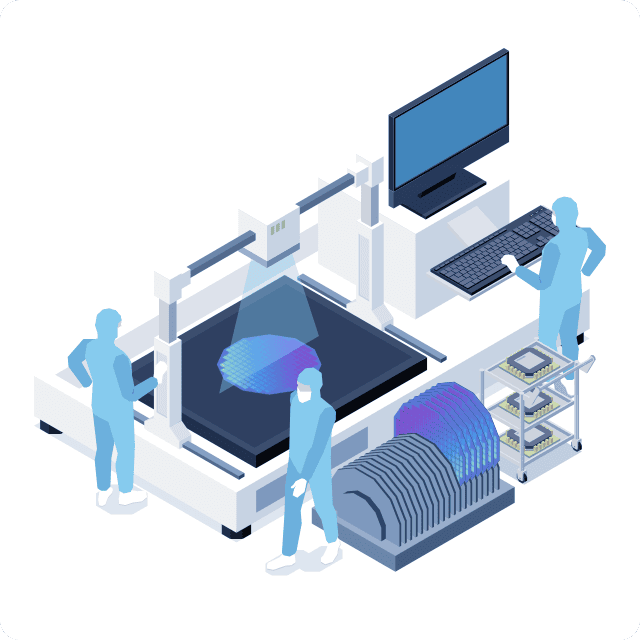
Sensing Device
Solutions

We develop semiconductor devices that solve data collection and security issues in the environmentally challenging field of sensing
Main industries served
- Consumer electronics manufacturers
- Industrial equipment manufacturers
- Healthcare equipment manufacturers
We will solve any problems you have with sensor device development!
-
Challenges in reducing costs
- Adopting generic products increases system construction costs
- Achieving the expected sensing capabilities with generic products is difficult
Best modularization proposal combined with low-cost generic products
- Modularization proposal combining customized sensor interfaces with low-cost generic products
- Further cost reduction by reducing the number of parts
-
Challenges in responding to end-of-life (EOL) products
- No ICs compatible with the system to replace EOL products
- Desire to improve security level beyond EOL products
Selecting the best manufacturing process and adding security features
- Achieve compatibility by adding logic as a replacement for EOL products
- Select devices that emphasize hardware security and improve security levels by adding features
-
Challenges in achieving miniaturization
- Portable, low-power systems are needed, but existing configurations have many limitations
Solar battery control and low power consumption design
- Ultra-low power consumption design and power shut-off enable construction of solar battery-powered systems
- Optimized battery control ensures product longevity
Main compatible devices
-
Customized differential output sensor IC
Special sensors customized to meet customer interface specifications
-
Solar cell LED control IC
LED control IC powered by sunlight with automatic dimming
-
Bio-sensor IC with ADC
Bio-sensor IC capable of analog-digital output
-
Image sensor IC
Image sensor that emphasizes hardware security
-
Microcontrollers equipped with next-generation memory
Microcontrollers equipped with ultra-low power consumption memory
Case Studies
-
Case study 01
Customizing special sensors to various interfaces to fit your products
Challenges before implementation
The sensor is special and does not match the interface of your product.

When launching a special sensor into the market, issues arose with interface specifications not matching due to the original power supply specifications. This made it difficult to launch the product in a timely manner.
Just ask NSW!
Proposing the best power supply systems and control logic to match special sensors to products

By designing a power supply system optimized for special sensors and customizing the control logic, we were able to meet the power supply specifications required for special sensors while ensuring compatibility with the product.
-
Case study 02
Reducing the number of parts, board costs, and system development workload through new IC proposal
Challenges before implementation
Combining multiple ICs increases board costs and system development workload

When using general-purpose ICs, it was necessary to combine sensor ICs and ADC ICs, which made it impossible to miniaturize the board, resulting in space and cost issues.
Just ask NSW!
Cost reduction and board miniaturization achieved by incorporating ADC and control logic into sensor IC

By proposing a sensor IC that combines a sensor, AD converter, and power supply system, we have achieved cost reductions by reducing the number of parts, miniaturizing the board, and reducing the burden of system development.
Development of image/audio processing devices

We develop semiconductor devices that solve issues such as high performance and tight deadlines in product development, enhancing the value of our customers’ products.
Main compatible products
- Image sensors
- Image processing equipment
- Audio processing equipment
We solve problems in image/audio processing device development!
-
Challenges for high performance
- Limited hardware resources
- High-speed operation required
Effective utilization of hardware resources
- Optimization of algorithms drawing on experience
- High performance through selection of the most suitable
-
Challenges in shortening delivery times
- Outdated design methods
- Verification becomes increasingly onerous as scale increases
High-level design methods, IP utilization
- Utilization of high-level design methods such as C language and MBD
- Greater efficiency through IP utilization
-
Challenges in power saving
- Increased power consumption due to larger design scale
- High difficulty to design power separation, etc.
Utilization of power saving design expertise
- Efficient power supply separation and clock stop design
- Power saving design by optimizing the operating speed
Main compatible devices
-
CMOS image sensors
LSI for image sensors combining analog and digital
-
Image processing engine for cameras
Improved image quality LSI with implemented algorithms
-
Image processing engine for medical equipment
High-resolution/high-definition image processing LSI for medical equipment
-
Audio Codec LSI
Codec processing LSI for portable audio
Case Studies
-
Case study 01
Achieving both circuit size reduction and image quality improvement in image processing for medical equipment
Challenges before implementation
Image quality improvement algorithm cannot be incorporated into FPGA

The implemented FPGA devices had limited circuit implementation scale, resulting in image quality issues. To make the product more competitive, it was necessary to resolve this issue.
Just ask NSW!
Balancing improved image quality and optimized hardware resources

We evaluated bit precision and explored optimal timing latency solutions using a software model, and successfully implemented the target image quality by trading off circuit scale.
Design flowchart
 Please scroll sideways to see
 -
Case study 02
Developing a large-scale image processing engine LSI with short turn-around-time (TAT)
Challenges before implementation
Development TAT does not match product cycle

Conventional design methods require the input of numerous engineers, especially for large-scale, short-deadline development projects. This makes it necessary to create vast amounts of documentation in plain language so that everyone understands the specifications, and it also leads to a decline in quality due to the large number of participants.
As a result, development TAT was prolonged and product launch was delayed.Just ask NSW!
Adoption of SystemC enables short TAT for large-scale development

For this case, we proposed SystemC. By creating specifications using the high-level design language SystemC, it was no longer necessary to create documents in plain language. At the same time, development was streamlined, enabling us to execute designs over 10 times larger than those created using conventional design methods. We also ensured quality through the utilization of verification IP and model-based methods.
SoC Development Solutions

We provide one-stop services ranging from consulting to high-quality design and verification for the development of SoCs suitable for application in a wide range of fields.
Main supported fields and products
- Semiconductor manufacturers
- Communication equipment manufacturers
- Industrial equipment manufacturers
- Included in /RISC-V core
- Included in various interface IP
- Included in image processing engine
We solve the challenges of SoC development!
-
Challenges in achieving high performance
- Hardware security against cyber attacks
- Highly complex system configuration, including selection of CPUs, bus configurations, and IPs appropriate for specific applications
Highly skilled in handling complex system configurations based on extensive experience
- Consulting services backed by our extensive experience
- Problem-solving capabilities drawing on our experience in developing a wide range of SoCs
-
Challenges in shortening delivery times
- Improvement of development methods to shorten product cycles
- Ensuring quality and responding to short TAT development
Capitalizing on a rich portfolio of Arm SoC development assets
- Leveraging long-standing collaboration with Arm to accelerate shift-left development
-
Challenges in power saving
- Achieving low power consumption in mobile-related products
- Increased power consumption due to high-performance processing in the AI field
Proposal of efficient power control design and hardware accelerators
- Efficient power separation and clock stop design
- Proposal of accelerators that replace software processing with hardware processing
Main Achievements
-
SoC for network control
XAUI/MⅡ/GMⅡ
5G/LTE/LTE-A/OFDM -
SoC for measuring instruments
LPDDR/PCIe/USB
/ Various serials -
SoC for automotive applications
(ASIL-D compliant)MIPI/DisplayPort
CAN/Various serials -
SoC for MFP
MIPI/DisplayPort/mini-LVDS
LPDDR/GbEther/USB/Various serials -
Object detection edge AI-equipped SoC for agriculture
MIPI/DisplayPort
LPDDR/PCIe/GbEther/USB -
SoC for IoT
BLE/Sensor/IrDA
ZigBee/Various serials
Case Studies
-
Case study 01
Shifting from microcomputers to custom product development that factors in PPA* * Performance/Power/Area
Challenges before implementation
Inability to develop customized products due to lack of expertise

When considering shifting from microcomputers to customized products, it was necessary to consider PPA. However, optimization of algorithms and the need for low power consumption posed challenges, and so there was no clear path forward.
Just ask NSW!
Achieving SoC development that emphasizes PPA

We proposed a coordinated design for converting software algorithms into hardware (considering not only performance but also compatibility with software) and combinations of various computing systems. This enabled the development of SoCs with an emphasis on PPA.
-
Case study 02
Upgrading SoC devices for higher functionality
Challenges before implementation
We want to upgrade products according to needs

We were asked to upgrade our products by incorporating AI and enhancing security. This required us to revamp the interface of our existing products and improve their processing capabilities.
Just ask NSW!
Product development tailored to customer needs

Drawing on our extensive experience in SoC development across a wide range of fields, we have developed products utilizing a variety of interfaces. We have also developed LSI for generative AI utilizing HBM, and achieved efficiency improvements by cutting back power consumption and utilizing memory tables.
Taking the above measures enabled us to increase the added value of the product.
Device test solutions
We provide one-stop support from device test specification review to mass production support, reducing test costs and improving operational efficiency
Main compatible products
- Automobile manufacturers
- Consumer goods manufacturers
- Industrial equipment manufacturers
We solve device testing challenges!
-
Challenges of enlarging devices and increasing functionality
- Increased testing costs due to longer testing times
- Quality assurance due to lower yield
Reduce device testing time, improve yield, and reduce testing costs while ensuring quality
- Optimize testing programs and change simultaneous testing measurements to reduce testing time
- Propose measures to improve yield by reviewing testing processes based on analysis of device testing results
-
Challenges in introducing semiconductor testers
- Lack of experience in introducing new semiconductor testers
- Lack of expertise in introducing semiconductor testers and converting programs from existing equipment
Seamless environment setup supported by engineers with a wealth of development experience
- Act as a bridge between semiconductor tester manufacturers and users to support the seamless launch of equipment environments
- Leverage extensive experience in program development to facilitate conversion to new semiconductor testers from various manufacturers
Main test solutions
-
Construction of device test environments
- Test program development
- Jig and tool creation
- Semiconductor tester startup
- Test program/pattern conversion
-
Mass production maintenance
- Yield improvement
- Test time reduction
- Fault analysis
-
Device testing
- Actual device operation/waveform verification
- Temperature characteristic evaluation
- Evaluation result analysis
-
Testing experience
Logic: Automotive, industrial equipment, LCD drivers
Memory: NAND, MRAM, FLASH
Analog: Automotive, industrial equipment, consumer equipment
Image sensors: Mobile, industrial equipment, consumer equipment
Case Studies
-
Case study 01
Migrating aging semiconductor testers to new semiconductor testers
Challenges before implementation
We would like to introduce a new semiconductor tester, but we are concerned about the measurement results

We were concerned about whether we could obtain equivalent measurement data before and after replacing the semiconductor tester.
In addition, we had little knowledge of the new semiconductor tester and did not have any engineers who could handle its start-up.Just ask NSW!
Solving issues in starting up new semiconductor testers

Based on our experience in semiconductor tester evaluation and bench evaluation, we conducted power/signal checks and correlation evaluations of the equipment, eliminating differences in measurement data before and after replacement.
-
Case study 02
Succeeded in yield improvement and test time reduction
Challenges before implementation
Yield decreased due to factory transfer

After the factory transfer, the yield of some products declined. However, improvement efforts did not proceed as planned because there was only a limited number of staff who could operate the semiconductor testers used.
Just ask NSW!
Program improvements have enabled improved yields and cost reductions.

We have extensive experience in coding and evaluating a wide variety of semiconductor testers.
In this case, we provided mass production data analysis, problem identification, and program improvement based on our expertise. Not only did we improve yield, but we also shortened test times and successfully reduced testing costs.
LSI turnkey service

From LSI development consulting to support
Even customers without specialist knowledge or resources can develop LSIs
Main compatible products
- New LSI development
- Recreation of EOL products
- Replacement from FPGA
- Analog LSI
- Mixed signal LSI
- Digital LSI
We solve LSI development problems!
-
Challenges in ensuring quality
- Quality assurance levels vary according to customer requirements
Proposals that emphasize cost-effectiveness
- Proposals tailored to quality assurance levels, such as full warranty, ESD only, replacement in case of failure, etc.
- Guaranteeing design quality as a TSMC’s DCA member
-
Challenges in saving power
- Increased power consumption caused by larger designs
- Lowering power consumption in mobile-related products
Accurate design utilizing various EDA tools
- Efficient power separation and clock stop design
- Accurate designs utilizing optimal tool chains
-
Challenges in achieving cost performance
- Increased costs due to scale expansion and enhanced performance
NSW proposes cost reduction
- Utilization of effective IP based on experience
- Selection of optimal Fab
- Utilization of overseas design houses
Main achievements
-
LSI for control systems
Process: 130 nm
PKG: 456 BGA
Cumulative MP: 6,000 -
LSI for control systems
Process: 65nm
PKG: 676BGA
Cumulative MP: 3,000 -
LSI for MFPs
Process: 0.35um
PKG: 208QFP
Cumulative MP: 186,000 -
LSI for security technology verification
Process: 65nm
PKG: 208LQFP
Prototype provided -
LSI for motor control
Process: 0.5um
PKG: 44LQFP
Cumulative MP: 147,900 -
LSI wafer supply for optical communication devices POC
Process: 7nm
Wafer provision
Case Studies
-
Case study 01
Responding to semiconductor device EOL by custom made copy
Challenges before implementation
We want to continue using EOL devices, but can’t find any alternatives

We wanted to continue using EOL products, but we couldn’t find any alternatives, and no manufacturer was able to handle small lots of around 10 units per year.
Even if a replacement product is available, there are times when it is necessary to review peripheral equipment due to differences in size or pin positions. We were looking for a replacement method that would keep costs down.Just ask NSW!
Custom made copy of EOL products with “Lite-ASIC” semiconductor mass production outsourcing service

At NSW, we are working with the Taiwan Design Center to create an environment where we can easily utilize the production capabilities of Taiwan Semiconductor Manufacturing Company Limited (TSMC).
For this case study, we fully customized an existing product and achieved pin compatibility with an EOL product. By outsourcing design and manufacturing to a Taiwanese company and having NSW manage the project, we were able to ensure quality even for small lots while keeping costs down. -
Case study 02
Delivering total solutions for development of prototypes equipped with cutting-edge technology
Challenges before implementation
It is necessary to find subcontractors for each process

Previously, it was necessary to find subcontractors with state-of-the-art technology for each process, starting from analog design and board design to LSI manufacturing and test design.
However, customers do not necessarily have expertise in all processes, so quality risks were expected to be high, making in-house management difficult.Just ask NSW!
Providing total solutions that cover all processes

NSW’s decades of experience and expertise in LSI design enable us to provide a one-stop service for all processes, resulting in enhanced quality.
We also proposed the optimal toolchain from each company’s EDA tools and provided cutting-edge, efficient designs.
In addition to supporting the provision of prototypes through strong alliances with major semiconductor manufacturers such as TSMC, our after-sales services, including LSI testing and board evaluation, have been highly rated by our customers.